Graphics Cards are equipped with the latest and the fastest memories around. The most popular and commonly used high-performance memory in budget-range, mid-range, and most high-end graphics cards is GDDR5 memory. GDDR5 has been around for quite some time and is used on many high-performance graphics cards. But the time is moving forward and technology is getting more and more advanced, and now we can see faster memories being developed that include GDDR5X, HBM, and HBM2 memory. Here in this post, I am going to tell you about all these high-performance graphics card memories and also compare them on the basis of physical and technical aspects.
Check out: Best Budget Gaming DDR4 RAM for Intel & AMD PC
GDDR5 Memory
GDDR5 is the most widely used high-speed memory that you see in the current generation of graphics cards. It is the successor of GDDR3 and GDDR4 memory. Nowadays GDDR3 or DDR3 is only used in entry-level graphics cards whereas GDDR4 is not even in existence anymore.
GDDR5 is one of the fastest graphics card memories and is used in many graphics cards starting from the budget, mid-range to high-end graphics cards. Some of the latest powerful graphics cards using GDDR5 memory are GTX 1060, GTX 1070, and Radeon RX 480. Budget and mid-range graphics cards using GDDR5 memory are GT 730, GT 740, RX 460, GTX 750 Ti, GTX 1050 Ti, etc.
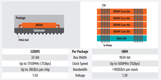
GDDR5 is a high bandwidth memory and has lower power consumption compared to its predecessors. It can reach speeds or has transfer rates of up to 8 Gbps. GDDR5 memory is manufactured by Samsung, Hynix, ELPIDA, or Micron, and GDDR5 memory chips are available in sizes of 512MB, 1GB, 2GB, 4GB, and 8GB. The bus width of each GDDR5 memory chip is 32-bits wide. The so-called successor of GDDR5 memory is GDDR5X memory which is even faster.
GDDR5X Memory
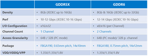
GDDR5X is an upgrade or improved version of the GDDR5 memory. Both GDDR5 and GDDR5X are high bandwidth SGRAM (synchronous graphics random access memory) that are used in graphics cards, high-performance servers, and other advanced hardware units. GDDR5X is twice as fast as the normal GDDR5 memory and can achieve speeds in the range of 10 – 14 Gbps. In the future, the memory speed of 16 Gbps can be made possible for GDDR5X. Currently, the GDDR5X memory is manufactured by Micron.
GDDR5X also consumes less power compared to GDDR5. GDDR5X memory chips are available in sizes of 4GB, 6GB, 8GB, and 16GB. The most popular Graphics Cards using GDDR5X memory includes GeForce GTX 1080 and Nvidia TITAN X (Pascal). High-end Workstation Graphics Cards such as Nvidia Quadro P5000 and Quadro P6000 also use high-speed GDDR5X memory. Samsung is planning to launch GDDR6 memory in 2018 which will be the real successor of GDDR5 memory. It will have speeds up to 16 Gbps, have lower power consumption, and will run at 1.35V only.
Note: It must be noted that in a PCB you cannot replace GDDR5 with GDDR5X memory because both have different pins. GDDR5 uses 170 pins per chip while GDDR5X uses 190 pins per chip.
GDDR6 Memory
GDDR6 is the successor of GDDR5 and GDDR5X. The memory will run at 1.35V and offer memory speeds up to 16Gbps (or up to 18GB/s) offering bandwidth up to 72GB/s. The memory is built on 10nm technology and will have a higher density of up to 32GB per die. GDDR6 is expected to make its way in the upcoming Volta / Turing based graphics cards from Nvidia. This super fast high bandwidth memory is aimed toward high-end gaming, virtual reality, cryptocurrency mining, and artificial intelligence (AI). GDDR6 is being manufactured by Samsung, Micron, and Hynix. Samsung and Micron GDDR6 will cater to the enthusiasts’ segment and will have a maximum speed of 16Gbps (16GB & 32Gb dies), while Hynix will offer their GDDR6 to the mainstream segment and will have speeds of 10-12 Gbps to 12-14 Gbps with 8GB dies.
GDDR6 memory is present in the Turing GPU architecture based workstation and gaming graphics cards from Nvidia that include Quadro RTX 8000, Quadro RTX 6000, Quadro RTX 5000, GeForce GTX 1660 Ti, GTX 1660 SUPER, GeForce GTX 1650 SUPER, GeForce RTX 2080 Ti, RTX 2080, RTX 2070, RTX 2060, Nvidia TITAN RTX, RTX 2060 Super, RTX 2070 Super, RTX 2080 Super, RTX 3070, RTX 3060 Ti. AMD Graphics Cards that use GDDR6 memory include Radeon RX 5500 XT, Radeon RX 5700, Radeon RX 5700 XT, Radeon 5600 XT, RX 6800, RX 6800 XT, RX 6900 XT.
GDDR6X Memory
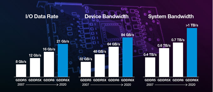
Currently, GDDR6X is the fastest graphics memory and delivers ultra-high bandwidth, which is close to that of HBM2 memory. GDDR6X is the successor of GDDR6 memory with significant improvements in all departments that include speed, bandwidth, and power efficiency. GDDR6X memory can have speed up to 21Gbps and can deliver bandwidth up to 1TB/s. The memory uses PAM4 signaling technology to achieve much higher speeds. It is developed by Micron and is currently being used in the latest top-end RTX 30 series graphics cards that include RTX 3090 and RTX 3080. These graphics cards are built on Nvidia’s latest Ampere GPU architecture.
HBM Memory
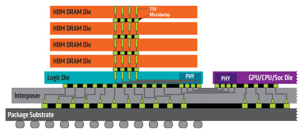
HBM stands for High Bandwidth Memory which is manufactured by Hynix and Samsung. It is also used in graphics cards and other advanced units. HBM memory is used in a few graphics cards as of now. HBM is a non-planar memory with a 3D design structure in the form of a cube or cuboid. In HBM multiple memory chips are stacked over one another to form a cube-like structure. This makes it occupies less space on the graphics card PCB and you can even put it close to the GPU. The change in the surface area also allows faster processing along with the chip.
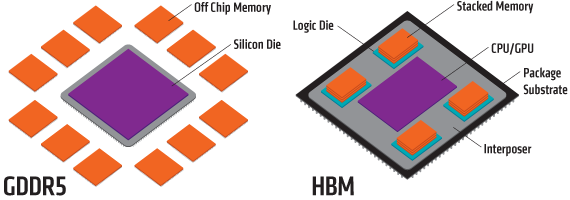
HBM memory is placed closed to the GPU in a graphics card PCB as shown below.
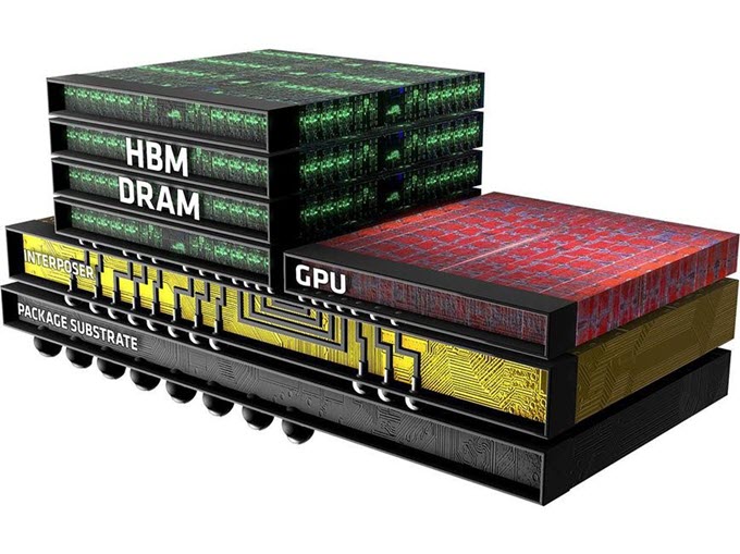
Each Stack of HBM memory is independent of the other stacks but they work together. HBM is also known as compact memory or stacked memory because of its small form factor. A normal HBM memory stack consists of four 4 DRAM dies on a base die and has two 128-bit channels per DRAM die making 8 channels in total which results in 1024-bit per stack of the memory interface. So a graphics card having four 4-Hi HBM stacks have a memory bus width of 4 x 1024 = 4096-bits. The operating speed of HBM memory is 1 Gbps but its memory bandwidth is much higher compared to GDDR5 memory. This is because of its much wider memory bus. The memory bandwidth of HBM memory can go as high as 128 GB/s per stack. HBM can have a 1 GB capacity per stack and supports 4GB per package.
HBM memory uses less power compared to both GDDR5 and GDDR5X memory. The first graphics card to use HBM memory was AMD Radeon R9 Fury X. It is also used in dual GPU graphics card Radeon Pro Duo.
Advantages of HBM Memory
- Lower Power Consumption
- Small Form Factor
- Higher Bandwidth
- Less heating
- Better Performance
Disadvantages of HBM Memory
- Expensive as of now
- Low availability as of now
HBM2 Memory
HBM 2 is the second generation HBM memory having all HBM characteristics but with higher memory speed and bandwidth. It can have 8 DRAM dies per stack and with transfer rates up to 2 Gbps. With a 1024-bit wide memory interface it can have a memory bandwidth of 256 GB/s per stack which is double the HBM or HBM 1 memory. The total capacity of HBM2 is also more and it can have up to 8GB per stack. The first GPU chip to utilize HBM2 memory is Nvidia Tesla P100. Nvidia’s latest Pascal series Workstation Graphics Card Nvidia Quadro GP100 also comes with HBM2 memory. HBM2 memory will be used mainly for VR Gaming, AR Gaming, and other heavy memory-intensive applications.
GPU architectures supported by HBM2 include Vega, Pascal, and the latest Volta GPU architecture from Nvidia. The successor of HBM2 is HBM3 which will be launched in 2019 or 2020. Some of the graphics cards that use HBM2 memory include Nvidia Titan V, Radeon Vega Frontier Edition, Radeon RX Vega 56, Radeon Vega RX 64, Nvidia Quadro GP100.
The 2nd generation HBM2 memory from Samsung is known as Aquabolt. It comes in 8GB HBM2 stacks (8-Hi height) with a speed of 2.4Gbps at 1.2V. It is much faster than the previous generation (first-gen) HBM2 memory that offered maximum speeds of 1.6Gbps @ 1.2V and 2.0Gbps @ 1.35V. This also means up to 50% additional performance over the first-gen HBM2 memory. It is also 9.6 times faster than the 8GB GDDR5 memory @8Gbps.
This second-generation Aquabolt HBM2 memory with a 1024-bit memory bus can deliver a bandwidth of around 307GB/s per 8GB stack, which is huge. You may see this 2nd gen HBM2 memory on next-generation high-end workstation graphics cards having up to 32GB memory capacity, which can offer about 1.2TB/s of enormous bandwidth. Samsung has achieved this performance with its new HBM2 memory by using new technologies in its TSV design (Through Silicon Via) and making tweaks to its thermal control. The new 8GB HBM2 single package will have 8 x 8GB HBM2 dies that vertically interconnect with over 5000 TSVs per die. Samsung has also added more thermal bumps between the HBM2 dies for better heat dissipation and it also acts as a protective layer at the bottom of the stack.
The third generation HBM2 memory from Samsung is High Bandwidth Memory 2E (HBM2E), codenamed as ‘Flashbolt’. It stacks eight 16Gb dies to achieve a single package capacity of 16GB, which is double compared to the previous generation HBM2 memory capacity (8GB). The 16GB capacity of HBM2E is achieved by vertically stacking eight layers of 10nm-class (1y) 16-gigabit (Gb) DRAM dies on top of a buffer chip. This HBM2E package is then interconnected in a precise arrangement of more than 40,000 ‘through silicon via’ (TSV) microbumps, with each 16Gb die containing over 5,600 of these microscopic holes.
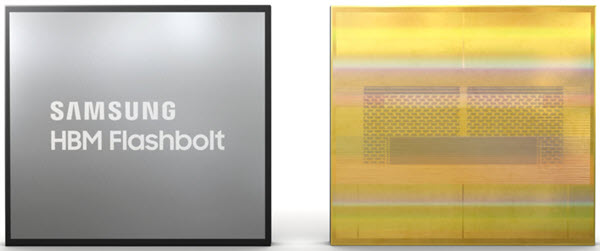
HBM2E operates 3.2Gbps and delivers a memory bandwidth of 410GB/s. It can also attain a much higher speed of 4.2Gbps (out of specs), delivering a bandwidth of 538GB/s, which is a 1.75X increase over the Aquabolt (307GB/s). HBM2E is designed for high-performance computing systems (HPC), and we can also expect it to see in upcoming high-end graphics cards. Along with increased performance, HBM2E is also very power efficient.
HBM3 Memory
HBM3 is an upcoming high-speed memory and the successor of HBM2 memory. HBM3 memory will be faster, have lower power consumption, and have increased capacity over HBM2 memory. HBM3 will allow up to 64GB VRAM on graphics cards and memory bandwidth of more than 665 GB/s and memory speed over 5.2 Gbps.
How to Calculate Memory Bandwidth
Use the below-mentioned formula to calculate the bandwidth of any type of memory.
Memory Bandwidth = (Effective Memory Clock x Bus Width) / 8
GDDR5 vs GDDR5X vs HBM vs HBM2 Memory
Here is neck to neck comparison of GDDR5, GDDR5X, HBM, and HBM2 memory types.
| Memory | GDDR5 | GDDR5X | HBM | HBM2 |
| Manufacturer | Samsung, Hynix, Elpida | Micron | Hynix, Samsung | Samsung, Hynix |
| Appearance | Square / Rectangular Chip | Square / Rectangular Chip | Cube / Cuboid | Cube / Cuboid |
| Maximum Capacity | 8GB per Die | 16GB per Die | 1GB per Stack | 4GB / 8GB per Stack |
| Maximum Speed | 8 Gbps | 10 to 14 Gbps (16 Gbps in future) | 1 Gbps | 2.4 Gbps |
| Bus Width | 32-bit per chip | 64-bit per chip | 1024-bit per stack | 1024-bit per stack or more |
| Power Consumption | Low | Same / Lower than GDDR5 | Lower than GDDR5 and GDDR5X | Lower than HBM |
| Graphics Cards Used in | Many Graphics Cards from budget, mid-range to high-end e.g. GT 740, GTX 1070, RX 480, etc. | GeForce GTX 1080, GTX 1080 Ti, GTX 1060, Nvidia Titan X (Pascal) | Radeon R9 Fury X, Radeon Pro Duo | Nvidia Tesla P100, Nvidia Quadro GP100, Radeon RX Vega 56, Radeon RX Vega 64, Nvidia Titan V, AMD Radeon VII |
See also:
- How much VRAM do you need in Graphics Card for Gaming
- Learn about CUDA Cores and Stream Processors in Graphics Cards
Final Words
In the end, I would like to say that all these above-mentioned memories are made for high performance and are used in high-performance hardware including top graphics cards. GDDR5 is the oldest of the lot while others are relatively newer. HBM2 is certainly the best memory in terms of performance and power consumption but it is very new and is not used in any commercial graphics cards as of now. You can expect to see the use of more HBM2 memory in the upcoming high-end graphics cards from Nvidia and AMD in 2018. If you have any queries or suggestions then you can connect with me by leaving a comment below.
(*This post may contain affiliate links, which means I may receive a small commission if you choose to purchase through the links I provide (at no extra cost to you). Thank you for supporting the work I put into this site!)


So performance wise GDDR5/X is better than HBM/2 and HBM/2 is better because of low power consumption. Right? and What about pricing? which one is cheaper?
HBM2 is better and expensive.
Well, no, HBM2 is better than gddr5/5X/6 in every aspect. The only problem (for the customers) is the difficulty to put GPUs and HBM memory on an silicon interposer…
What do you recommend on a gtx 1080and Vega 56 in terms of speed in 3d applications and low power consumption
You mean between these two?
Which is better GTX 1080 or RTX 2070?.
Well its too early to say but i think RTX 2070 is faster and better than GTX 1080.
Ddr5x or ddr6 is the future. Amd is trying to be far to exclusive with their tech, just like nVidia is with Ray tracing and dlss nonsense. When these two companies join technology, life on earth will be in sync.
I agree with you as both of them are going their own way, creating more chaos and confusion among users and also game developers.
Ddr4 or gddr 4
How is corect ?
I know ddr is for ram memory and gddr is for video memory but I saw it written in both ways
GDDR4 was shortly lived but you can still find DDR4 in some entry level graphics cards e.g. GeForce GT 1030 (DDR4 variant).
Performance is spelled wrong under the advantages of HBM portion of the blog
Typo corrected. Thanks for letting us know.
Which one would you opt for: 8GB GDDR5 or 6GB GDDR6? Thanks.
Well, it really depends on the type of usage but I would prefer more RAM as GDDR5 is fast too.
8GB GDDR5 is also likely on a wider bus… so they probalby have about equal bandwidth.
hi this is my first time writing about a video card which I have is a r9 390x with 8gb which now I have it for 2 years and very happy with it im a self tought tech on hardwares on pc but my card was over heating at 94c full load and found out that I had to clean the vents and reclean and paste the gpu which I found it was very weak from mfg now it running at 47c when its cold here but in the summer it runs at 63c I also turn down the specs from 1015mz core to 815mz then the mem at 1500mz to 1000mz because because if I run it at full mfg spects it will run at 87c to 90c now do I lose a lot by running lower spec that the card was made for? its just im scare for the heat unless the card was made to run hot at top specs
R9 390X does run very hot and I think it is normal for it to run at 87C to 90C at full load.
Can you comment on Fujitsu A64FX now using HBM2 ?
Is 1080ti better than 2070 Super?
It is slightly faster but RTX 2070 SUPER consumes less power and comes with RT cores and Tensor cores for Real Time Ray Tracing and DLSS (Deep Learning Super Sampling).
I believe the listed capacities are wrong, Gb should be used instead of GB. Well Gib if you want to be technical but that’s a small distinction
For HBM/HBM2 GB per stack and Gb per die is correct.
Excellent article, Thank You.
Who owns the patents on HBM, HBM2, HBM3?
HBM memory was first produced by SK Hynix.
Dear Akshat Ji,
can i get your mobile no.
Thanks
Tushar
Sorry, but you can contact me on facebook.